Presentation
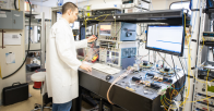
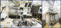
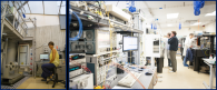
PhotoNext is a competence center on Applied Photonics launched by POLITO in summer 2017 as one of its strategic research efforts, and received 1.8 M€ of funding of for three years. These funds will allow purchasing new large experimental equipment thus establishing the PhotoNext center at top-level international state-of-the-art in experimental capabilities.
The EU Horizon2020 roadmap recognizes Photonics as a Key Enabling Technology (KET), and PhotoNext fits perfectly in the EU Photonics Work Programme, by focusing its activities on three main areas:
- Action A1: Ultra-high speed optical networks for next-generation ultra-broadband optical communications
- Action A2: New optical sensors for safety, industrial, civil and life science applications
- Action A3: Optical components with innovative functionalities to generate, manipulate and detect light
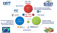 PhotoNext researchers have recognized expertise and international positioning on topics (A1) and (A3), the two being so far independently developed. The PhotoNext strategy is to combine and integrate the skills and know-how to develop advanced optical components for next generation telecommunication networks and industrial applications. Moreover, PhotoNext will create a new competence centre for POLITO on topics (A2) by extending its expertise on optical sensors to several applications, ranging from aerospace to environmental sensing, from structural health monitoring to biomedicine.
The three areas targeted by PhotoNext are undergoing major revolutions. As an example, in 2016 the major telecommunication operators started to massively substitute the old “copper based” telephone network with new optical fibers for ultra-broadband access networks, with resulting strong social impacts in large and medium cities. PhotoNext will allow POLITO to be a key leader in this forthcoming trend, also considering another ongoing revolution: the “optical cloud” is being deployed everywhere in our cities and may enable completely new applications, based on pervasive distributed optical sensors. The new instruments acquired will allow PhotoNext to perform top-level experimental activities in the never-ending rush toward increasing the speed and reach of optical fiber transmission systems, strengthening the industrial collaborations with key vendor and operators of this field.
Another undergoing revolution is happening in optical components covering several application fields:
- Optical fiber based components have proved to be the backbone of the internet revolution and are finding new applications when optical fibers can integrate different functions, enabling compact and efficient devices so far unconceivable. Examples include multicore optical fibers for ultra-broadband transmission, multimaterial fibers combining optical stimulation with electrical signal detection, fiber laser sources with integrated sensing capabilities for materials processing and functions for release of chemicals where appropriate, bio-resorbable fibers for diagnosis and therapy of tumors.
- Planar components are experiencing the “silicon photonic” revolution, which has the potential to reduce the cost of photonics bringing it to the level of electronic components in silicon.
PhotoNext will also develop new types of optical sensors and extend their use to very different fields, such as: system monitoring in aerospace, railways and automotive sectors; environmental monitoring of the territory, such as for landslide and avalanche prevention; remote sensing for security and civil applications.
All PhotoNext activities are carried out by multidisciplinary research groups where engineers working in the fields of electronics, telecom, materials, transports and mechanics, and geophysics team up to achieve new outcomes which will greatly benefit the scientific community, the collaborating companies and the Society.
You can find here a video describing the main features of the Center: